High-Standard Electromagnetic Compatibility (EMC) Design of Telecom Rectifier Systems for Effective Resistance to Strong Electromagnetic Interference

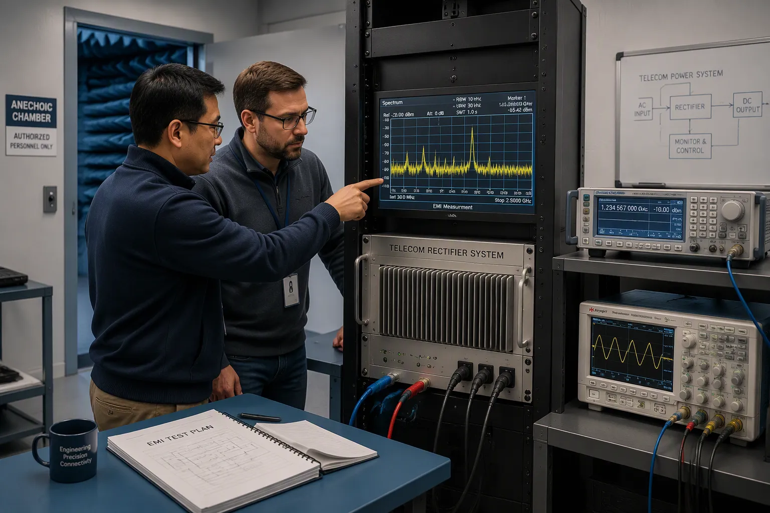
You cannot bolt electromagnetic compatibility onto a finished power supply. Good design starts with three principles: suppress noise at the source, control the coupling path, and harden the system against incoming disturbances. Think of it as EMC by design, not by afterthought.
Strong interference — lightning surges, electrical fast bursts, radiated fields, conducted noise, and fast switching transients — can upset control circuits, damage components, and interrupt service. Telecom Rectifier Systems sit at the heart of that risk, so their immunity directly protects network uptime.
This post gives you concrete design techniques, standards references, test methods, and cost-performance guidance. ESTEL appears throughout as an example design and supply partner.
Key Takeaways
Design EMC into the rectifier from the beginning, not as an afterthought.
Suppress noise at the source, control the coupling path, and harden the system against disturbances.
Use filtering, shielding, and grounding together to block interference.
Test early with pre-compliance checks to catch problems before formal certification.
Budget extra margin below emission limits and above immunity levels to stay compliant over time.
Strong EMI Threats and EMC Standards for Telecom Rectifier Systems
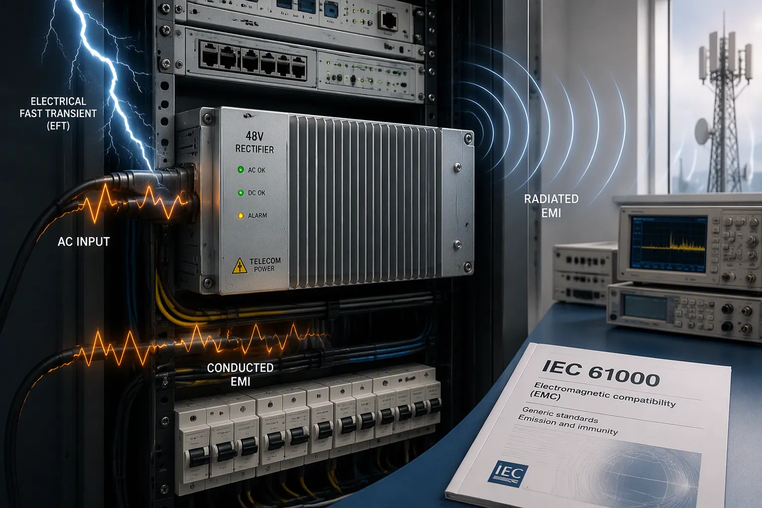
Characterizing Strong EMI Threats
You need a clear picture of what threatens a rectifier before you can design against it. Telecom sites expose power equipment to several distinct disturbance types, and each one couples into the system differently.
Lightning surges arrive on AC mains and on outdoor DC or signal cabling. A nearby strike induces large transient voltages that stress input rectifiers, filter capacitors, and control boards. Switching transients form a second threat. Grid switching, capacitor bank operations, and contactor arcing produce fast bursts of high-frequency energy. Radiated fields from nearby transmitters, base station antennas, and other equipment couple into enclosures and cables. Conducted disturbances travel along AC mains and along the DC output bus, where they can reach sensitive load equipment. Fast switching transients inside the rectifier itself — from MOSFET or IGBT commutation — add another layer of internal noise.
These threats interact with Telecom Rectifier Systems in ways that matter for service continuity. A surge can destroy a semiconductor junction in one event. Repeated bursts can degrade insulation and filter components over time. Conducted noise on the DC output can disturb downstream telecom loads even when the rectifier keeps running. Treat each threat as a design input, not an occasional nuisance.
Key Standards and Compliance Targets
Standards give you a common language for measuring and limiting these threats. The IEC 61000 series forms the backbone. Its immunity parts define test waveforms and severity levels for surges, electrical fast transients, electrostatic discharge, conducted RF disturbances, and radiated fields. Its emission parts set limits on what your rectifier may inject back onto the mains and into the environment. CISPR 32 and its European counterpart EN 55032 cover emission requirements for multimedia and information technology equipment, and many telecom power supplies align with them. IEC 61000-6-2 and IEC 61000-6-4 provide generic immunity and emission targets for equipment in industrial environments.
Telecom-specific frameworks add another layer. ITU-T K.20, K.21, K.44, and K.45 address surge withstand for equipment connected to telecom networks, and they define test setups that reflect real installation conditions. Regional schemes such as the CE marking route in Europe and FCC Part 15 in the United States complete the picture.
The value of these documents lies in their uniformity. Every lab applies the same surge waveform, the same burst repetition pattern, and the same field strength calibration. You can compare results across suppliers and across design revisions. Compliance targets then become concrete: pass the immunity tests at the specified severity level, and stay under the emission limits with margin to spare. That shared method is what makes EMC a controllable engineering discipline rather than a matter of luck.
EMI Filtering Design
Filter Topologies and Components
A well-built input filter uses several stages. A common-mode stage with a current-compensated choke and Y-capacitors blocks noise that travels on both lines in phase. A differential-mode stage with X-capacitors and a choke handles noise between the lines. Output filtering follows the same logic on the DC side, where you protect downstream telecom loads from switching residue.
You can choose passive or active control techniques. Passive filters absorb unwanted energy with capacitors, resistors, inductors, and transformers. They suit large signals, need no auxiliary supply, and often cost less. Active filters detect the disturbance and inject a canceling current. A hybrid approach combines both: one transformerless active circuit added to a passive filter gave over 10 dB of extra reduction on a 50 W DC-DC converter at full load, with more than 30 dB in the 300–500 kHz range and about 10 dB near 7–30 MHz.
Damping and Insertion Loss
Insertion loss measures how much a filter attenuates a signal. Per the CISPR 17 test setup, insertion loss = 20·log(V20 / V2), where V20 is the load voltage without the filter and V2 is the voltage with it. A high number sounds reassuring, yet a realistic source and load simulation can show insertion gain instead — noise rising by more than 10 dB near 200 kHz. That gain can upset conducted emissions and destabilize the control loop, so find it early.
Damping tames the resonance peak. Add a capacitor (Cdamp) in parallel with the input capacitor, paired with a loss element (Rdamp) chosen for a quality factor of roughly 0.5–0.8. Keep the filter inductance low so Q stays controlled. Remember that source impedance shifts the resonance, and constant-power loads present negative incremental impedance. Model differential mode against a ~100 Ω load and common mode against ~25 Ω, not the idealized 50 Ω datasheet condition. Verify with a LISN, probes, and impedance measurements before production.
Shielding and Enclosure Design
Enclosure Materials and Seams
Your enclosure is the last barrier between internal switching noise and the outside world. Choose a conductive metal — steel or aluminum — for the main structure. Paint and anodizing look good, yet they insulate the surface and block bonding. Mask contact areas, or use conductive finishes at every seam.
Seams and apertures leak more than solid walls. Bond mating surfaces with conductive gaskets along the full perimeter. Keep vent and window openings much smaller than the wavelength of the highest frequency you must block. Honeycomb waveguide vents bonded around the perimeter and conductive mesh laminated into glass or plastic handle this job well.
Cable Shielding and Feedthroughs
Cables act as antennas. Terminate each shield 360° at the connector shell or enclosure entry point. Long pigtails add inductance and turn the shield into a radiator. Use shielded connectors with full circumferential contact, and bond metal backshells directly to the panel. Painted or anodized bonding surfaces are a common leakage point.
Practice Area | Recommended Practice |
|---|---|
Grounding strategy | Both ends grounded for high-frequency performance; single-end grounded to avoid ground loops at low frequency |
Shield material | Braid for hundreds of MHz; foil above 100 MHz; braid plus foil for wideband |
Feedthroughs | Terminate shields 360° to the enclosure wall at entry; use filtered connectors |
Every penetration must pass through all shield layers with filtering at each layer. Verify bonding with continuity testing — DC resistance of 2.5 mΩ or less between panel and case — and confirm attenuation per IEEE 299 or MIL-STD-285.
For cable shielding effectiveness, ANSI/SCTE 48-3 specifies a GTEM cell procedure for 75-ohm braided coaxial drop cables and connectors. IEC 61726 covers screening attenuation using reverberation chambers. Transfer impedance testing links shield current to the disturbance on the protected side, and it remains a key measure for cables, connectors, and conduits.
Grounding Architecture
Single-Point vs. Multi-Point Grounding
Grounding choices shape how noise currents flow through your rectifier system. Single-point grounding ties all returns to one reference node. This approach works well at low frequencies, where the connection behaves like a true short circuit. It also suits mixed-signal layouts, because it stops low-frequency currents from sharing paths with sensitive circuits.
Multi-point grounding bonds each return to a common plane at many locations. Short, wide connections keep impedance low at high frequencies, where a single long conductor starts to look like an inductor. This approach fits digital boards, chassis-level bonding, and any design with fast switching edges. Many telecom rectifiers combine both: a multi-point chassis plane for high-frequency currents, plus a single-point tie for low-level control signals. Match the method to the frequency range you must control.
PE, Chassis, and Signal Bonding
Bonding practice follows a clear hierarchy. The building ground electrode system anchors everything. A telecommunications main grounding busbar (TMGB) ties to it through a 3/0 AWG bonding conductor kept within 4.5 m. Zone-level telecommunications grounding busbars (TGB) sit below the TMGB, and equipment grounding conductors run from each rack or chassis to those bars. The telecom ground is supplemental — it bonds to the same earth electrode but does not replace the equipment grounding conductors required by NEC Article 250.
Bonding Element | Recommended Practice |
|---|---|
Rack rails | Bond with #6 AWG conductors; keep runs to the TGB or TMGB short, typically under 1 m |
Cable tray | Bond at intervals not exceeding 3 m |
Equipment chassis | Direct chassis bond via mounting hardware; verify chassis-to-TMGB AC voltage below 1 V RMS |
TMGB copper bar | ETP copper, minimum 6 mm thick, typical 600 × 200 × 6 mm, 6 mm holes on 25 mm centers per EIA/TIA 607 |
Verification | Ground electrode resistance ≤ 5 Ω; bond resistance ≤ 0.1 Ω |
Rack-mount telecom power systems often use a copper bar for grounding protection. The bar gives every module a short, low-impedance path to the reference. Verify each path with a micro-ohmmeter and confirm continuity from rack to TGB and TGB to TMGB before you energize the system.
PCB Layout for EMC
Loop Areas and Layer Stackup
Radiated emissions scale with loop size and current slew rate. Enclose every switching loop — high-side drivers, MOSFETs, and their return paths — in the smallest possible area. Group associated components tightly to shorten traces, and the return path shrinks with them. Route high-speed nets directly over a continuous ground plane, and never cross a plane split. Add ground vias tightly around signal vias at every layer transition so the return current stays close to the forward trace.
A deliberate stackup does much of this work for you.
Technique | EMC Benefit |
|---|---|
Dedicate inner layers to power and ground returns | Clean reference and return paths |
Place power planes adjacent to ground planes | Interplane capacitance filters high-frequency noise |
Sandwich signal layers between planes | Shields signals and reduces crosstalk |
Balance copper distribution per IPC-6012 | Prevents warpage and maintains flatness |
Keep signal layers close to ground layers with thin dielectrics. Use thicker dielectrics between signal layers to control crosstalk, and verify impedance profiles by simulation. Bridge any unavoidable plane split with stitching capacitors to give high-frequency content an AC return path.
Isolation and High-dv/dt Nodes
High-dv/dt nodes are your loudest on-board noise sources. Keep switch node copper small, and place snubbers to dampen transients. Add guard rings around noisy components to divert stray fields. Place input and output filters at board edges to block differential-mode noise at the boundary. Use ferrite beads on cables, and apply orthogonal routing so adjacent traces do not couple.
Isolation spacing protects sensitive circuits from these aggressors. Maintain the creepage and clearance your safety standard requires between primary and secondary, and keep control and sensing traces away from switching nodes. Confine differential pairs tightly so the field stays between the traces. Separate quiet analog references from power return currents, and give each its own return path back to the source.
Component Selection for Telecom Rectifier Systems
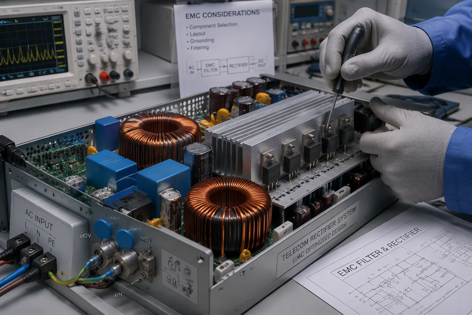
Semiconductors, Magnetics, and Capacitors
Component choice sets the EMC floor of your design. Pick parts that tolerate stress and generate less noise, and the filter and shield have less work to do.
For power semiconductors, favor devices with controlled switching edges and low parasitic capacitance. Soft-switching topologies reduce dv/dt and di/dt at the source, which lowers both conducted and radiated emissions. Choose MOSFETs and IGBTs with rugged gate structures and adequate voltage margin for surge events. Thermal headroom matters too, because a hot junction degrades switching behavior over time.
Magnetics deserve equal care. Use high-permeability cores for common-mode chokes, and select core material that holds its properties across your operating temperature range. Powder cores suit differential-mode chokes where saturation current is high. Wind chokes with balanced, symmetrical windings to keep common-mode rejection strong.
Capacitors split into two jobs. X-capacitors handle differential-mode noise across the line, and Y-capacitors divert common-mode current to ground. Choose film or ceramic types with low equivalent series resistance and stable capacitance over temperature. Derate voltage generously, since surge events push capacitors well past nominal stress.
Protection Devices and Qualification
Protection devices form the last line of defense. A well-equipped rectifier includes several layers:
Surge protection at the AC input, with metal-oxide varistors or gas discharge tubes rated for the surge current your site expects
Built-in overvoltage, overcurrent, and overtemperature protection circuits
Short-circuit protection with automatic recovery for long-term reliability
Robust construction and a wide operating temperature range for harsh sites
Qualification separates a reliable part from a risky one. Screen every candidate against recognized criteria:
Category | Recommended Criteria |
|---|---|
Certifications | UL, CE, TUV, RoHS |
Industry standards | IEC 62368, TIA-569-C, GR-1089, 3GPP |
Checklist items | Voltage and current ratings match system requirements; certification from recognized bodies; adherence to environmental and safety regulations |
One well-fitting example is ESTEL's Telecom Rectifier System. It delivers a DC48V output with current options from 6A to 125A, and efficiency exceeds 96%. The 6U, 3U, and 2U rack-mount designs fit standard 19-inch racks. A modular layout supports scalability and maintenance, and a copper bar provides grounding protection. The platform also aligns with transient-voltage protection and electromagnetic interference standards, which supports clean integration into telecom infrastructure. Treat it as one option among several, and compare candidates on the same checklist.
Testing and Validation
Pre-Compliance Testing
You should test early and often, long before you book a certified lab. Pre-compliance testing happens in your own facility with bench equipment that approximates the official setup. A LISN on the AC input, a near-field probe, a spectrum analyzer, and a TEM cell or GTEM cell cover most conducted and radiated checks. These tools will not match a certified chamber, yet they reveal trends and catch gross failures while changes remain cheap.
Auxiliary circuit transient testing deserves a place in this early phase. Fast switching transients from your own converter can upset control and protection circuits even when the main power stage passes. Inject fast edge pulses into the auxiliary supply, the gate driver, and the sensing lines, then watch for false trips or logic errors. Repeat the test across the full input voltage range and at temperature extremes. Fix weak spots at the bench, and you avoid a costly redesign later.
Compliance Testing and Margin
Formal compliance testing follows the standard methods you designed against. An accredited lab applies the IEC 61000-4 series waveforms for surges, bursts, and radiated fields, and it measures emissions against CISPR limits. Book this test with time to spare, and bring a unit that already passed your in-house checks.
Budget margin on purpose. A design that squeaks past the limit at the lab will drift out of compliance as components age, as production tolerances shift, and as the next revision changes the layout. Aim for a comfortable gap below the emission limits and above the immunity levels. Treat the standard limit as a floor, not a target. This margin strategy protects Telecom Rectifier Systems across their service life and keeps field failures rare.
Implementation and Cost Trade-Offs
Balancing Cost and EMC Margin
Every EMC decision carries a price tag. Extra filter stages, shielded cables, and conductive gaskets all add to the bill of materials. You face a real tension between keeping unit cost low and keeping margin wide. Resolve it by ranking each measure against the risk it retires.
Invest first where a failure would cost the most. Input surge protection and a solid common-mode filter stage protect against the threats that destroy hardware outright. Shielding and layout refinements usually cost little and deliver broad gains. Spend on premium connectors and gaskets last, once the fundamentals are sound. A cheap fix at the source often removes the need for an expensive fix downstream.
Track margin as a design parameter, not a final surprise. Record the gap between your measured emissions and the limit at each prototype build. A shrinking gap signals rising cost later, because late fixes demand rework, retesting, and schedule slips. Early spending on a better choke or a cleaner layout usually beats emergency spending after a failed lab run.
Design Reviews and Partner Collaboration
Schedule design reviews at every major milestone. Bring layout, magnetics, and enclosure drawings to the table together, because EMC problems often live at the boundaries between them. Invite a reviewer who has not lived with the design. Fresh eyes catch shared return paths and unshielded seams that the original team stopped seeing.
Iterate on prototypes with purpose. Build a unit, test it at the bench, fix the weak points, and build again. Each cycle should retire a specific risk rather than confirm what you already know. Document every change and its measured effect, so the next revision starts from evidence.
An experienced partner can shorten this loop. ESTEL supports design review, cabinet integration, and test validation for Telecom Rectifier Systems, and its modular rack-mount platforms give you a proven starting point for 19-inch installations. Compare partners on their review process and test support, then choose the one that fits your program.
You now have a complete EMC strategy. Suppress noise at the source with soft switching and tight component choices. Control the coupling path through filtering, shielding, grounding, and careful PCB layout. Validate early with pre-compliance testing, and budget margin deliberately so your design stays compliant as parts age and revisions accumulate.
Treat EMC as a first-class requirement from concept through certification. Give it budget, schedule, and review time alongside every other specification. Experienced partners such as ESTEL can support design review and validation for Telecom Rectifier Systems, and that collaboration helps you reach certification with confidence.
FAQ
Which EMC standards should I design against first?
Start with the IEC 61000 series. Its immunity parts define surge, burst, ESD, and RF test waveforms. Its emission parts set limits on what your unit injects back onto the mains. Add ITU-T K.20 and K.21 for telecom surge withstand, plus CISPR 32 for emissions. These documents give you uniform test methods you can design and verify against.
How much EMC margin should I budget?
Treat the standard limit as a floor, not a target. Aim for a comfortable gap below the emission limits and above the immunity levels. Components age, production tolerances shift, and each revision changes the layout. A design that barely passes at the lab will drift out of compliance over its service life.
Where does filtering stop and shielding begin?
They solve different problems, so you need both. Filtering blocks conducted noise on the AC input and DC output. Shielding contains radiated fields and protects cables and seams. Grounding and layout tie the two together. Fix noise at the source first, then let filtering, shielding, and grounding handle what remains.
What should I check before booking a compliance lab?
Run pre-compliance tests in your own facility first. Use a LISN, near-field probe, and spectrum analyzer to catch gross failures while changes stay cheap. Inject fast transients into auxiliary circuits and gate drivers. Confirm bonding continuity from rack to grounding busbar. Bring a unit that already passed your in-house checks.
How do I choose a rectifier platform for a high-EMI site?
Compare candidates on the same checklist: certifications, surge protection layers, filter topology, grounding practice, and test evidence. ESTEL's Telecom Rectifier Systems offer one well-fitting option, with DC48V output, 6A to 125A models, efficiency above 96%, 6U/3U/2U rack-mount designs, and copper bar grounding protection.
See Also
Ensuring Consistent Power Supply for Telecom Cabinet Operations
Advantages of Lithium Batteries Over Other Telecom Cabinet Options
Key Features to Consider in Telecom Power Supply Systems
Grid-Tied Solar Inverter and Battery System for Telecom Cabinets
Comprehending Global Standards for Communication Power Supply Equipment
CALL US DIRECTLY
86-13752765943
3A-8, SHUIWAN 1979 SQUARE (PHASE II), NO.111, TAIZI ROAD,SHUIWAN COMMUNITY, ZHAOSHANG STREET, NANSHAN DISTRICT, SHENZHEN, GUANGDONG, CHINA
